S.I.T. focuses on preparing engineering graduates for careers in semiconductor design through domain-focused VLSI training.
The institute’s approach is centred on helping students move beyond academic theory and develop practical understanding of semiconductor design workflows used in the industry.
Training is structured around specialised domains such as
Physical Design, Design Verification, and Analog Layout enabling students to build focused expertise aligned with industry roles.
Courses Completed
Happy Students
Class Strength
Unlike generic electronics training, S.I.T. structures its programs around specific semiconductor design domains.
Students learn the concepts, workflows, and engineering practices relevant to their chosen domain, helping them develop deeper understanding of how semiconductor design teams operate.
Domain-focused learning allows students to build specialised skills that align with real engineering roles in chip design teams.
The curriculum is designed to reflect the workflows used in semiconductor design environments.
Students learn how different stages of chip development connect — from design concepts to verification and implementation. This approach helps students understand not only the technical concepts but also how semiconductor engineering teams collaborate throughout the design process.
The focus is on building practical understanding rather than purely theoretical knowledge.
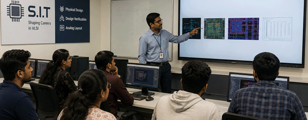
Practical exposure is an important part of semiconductor training.
All students at S.I.T. undergo a 6-week internship exposure, allowing them to observe and understand real-world semiconductor design workflows and engineering environments.
This experience helps students connect classroom learning with practical engineering practices used in semiconductor development.
Semiconductor design involves specialised engineering tools used across chip development teams.
Training at S.I.T. introduces students to environments used in modern semiconductor design ecosystems, including platforms from Cadence, Synopsys, and Mentor Graphics.
Exposure to these environments alongside domain concepts helps students better understand how semiconductor design teams operate.
S.I.T. training is structured to help students build a progressive understanding of semiconductor design.
Understanding semiconductor design concepts
Developing domain knowledge in a chosen specialization
Gaining exposure to design workflows used in the industry
Building confidence in applying domain knowledge to engineering problems
This structured learning approach helps students prepare for entry-level semiconductor design roles.
S.I.T. training is guided by experienced faculty with backgrounds in semiconductor design and related engineering domains.
The faculty team focuses on helping students understand both conceptual foundations and practical engineering considerations involved in semiconductor development.
Through mentorship and guided learning, students receive support in building the knowledge required for specialised semiconductor roles.
S.I.T. focuses on creating a learning environment where students can concentrate on building domain expertise in semiconductor design.
By focusing on specialised domains rather than broad electronics topics, the institute aims to help students develop clarity about career pathways within the semiconductor industry.
Students exploring semiconductor careers often have questions about domains, roles, and industry expectations.
S.I.T. provides guidance to help students understand:
This helps students make informed decisions about their learning path.